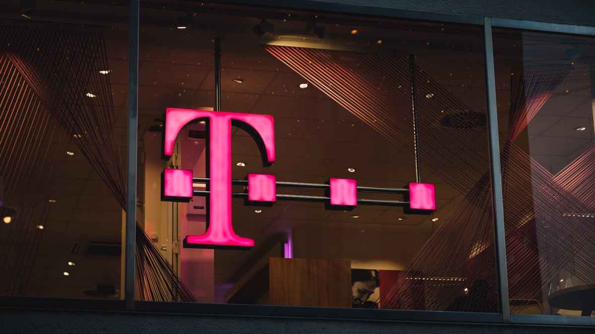
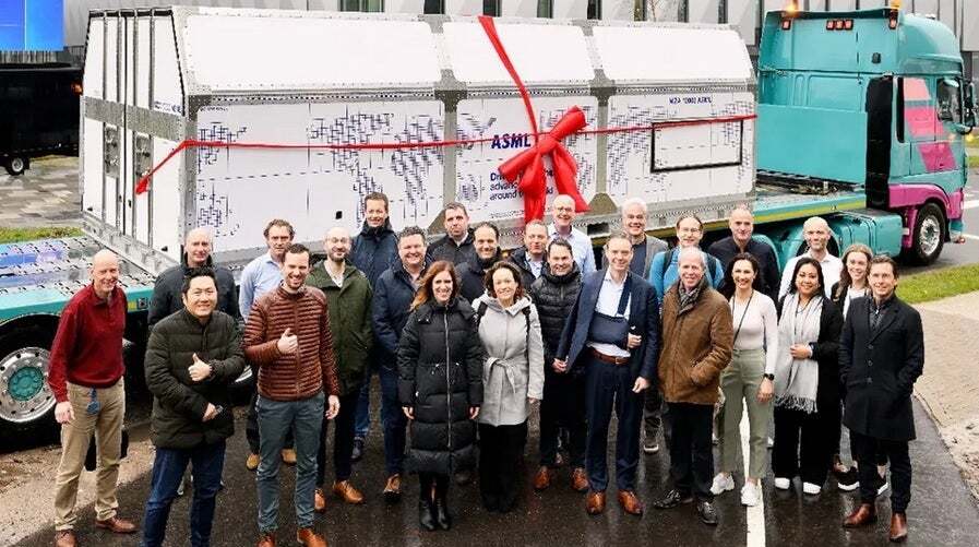
[ad_1] The new EUV machines are not made by the Dutch company ASML, and the Intel was the first muse to receive new machines. It provides an increase in the digital aperture (which NA in the name of the device) to. This allows the nobility to build chips using the under 3nm practical nodes. Low nodes are usually used as smaller transistors, which means that more important "building blocks" can be copied within a specific area of an integrated circle. The density of the higher transistor makes a more powerful slice and/or energy efficiency. The new high -NA machines need a fewer exposure to printing designs on silicone chips that allow Intel to save time and money. What previous EUV machines took three exposure and approximately 40 processing steps that can be taken with high NA machines with only one exposure and one number one of the processing steps. ASML staff stands in front of a box that has a highly combined stone printing machine between EUV before shipping to Intel. | Credit image Yesterday, Intel said at a conference in San Jose, California that the first intense machines I bought in production, which means that it is used in the process of making chips. Intel says that new machines are about weak reliability of the original EUV machines. According to the main main engineer of Intel Steve Carson, his company produced 30,000 chips (each chip can contain thousands of chips depending on the return) using high -size stone printing machines. "We are getting chips at a consistent rate, and this is a huge blessing for the platform," says Carson. Intel Foundry Services (IFS) seeks to restore driving from TSMC and Samsung Foundry. The Intel's A18 knot, which is scheduled to start the huge production in the second half of this year, resembles the TSMC and Samsung Foundry 2NM knots, both of which will also start huge production in the second half of 2025. Intel has a short window of opportunities since then since then Then this will be the only cause using the BSPD (BSPD) feature that connects It has energy for several months. This feature moves the power wires to the back of the chips, which leads to a more efficient power to the chip transistors, allowing them to run at higher speeds. TSMC plans to include rear energy delivery using a 2nm node (N2P) specified for huge production next year. Intel lost the driving of the operation when the company took seven years before the feeling that it could rely on the EUV stone printing, allowing TSMC and Samsung to overcome it. In addition, Intel has partially confronted chips in 10nm due to its dependence on old stone printing equipment. The decision to jump quickly to buy high EUV machines notes that she does not want to make the same mistake twice. The NA EUV is used to help produce chips using the Intel 18A operation knot. This will be used on the Panther Panther Lake with a chip that will be customized for use on laptops. New stone printing machines are expected to get a severe exercise when Intel begins using them for a 14A node. There is no date for a tangled production yet for that knot.High stone printing machines require less time and money to convert circles patterns into silicon chips
After waiting for seven years to use OG EUV machines, INTEL lost the leadership of TSMC and Samsung Foundry process
[ad_2]
Download
Seeking to regain process leadership from TSMC, Intel refused to make the same mistake twice
Almost a year, Intel released a video showing that the company is receiving $ 400 million from EUV devices, the second generation of ASML extremist ultraviolet printing machines. The original EUV was the indispensable tool that your chips needed to take the process of the process under 7nm. Stone printing machines help transfer circuit patterns on silicone chips that are the basis for chips production.
| Name | |
|---|---|
| Publisher | |
| Genre | News & Magazines |
| Version | |
| Update | February 25, 2025 |
| Get it On |  |